The Pribiag group's research applies innovative nanofabrication and low-temperature measurement techniques to uncover the electronic properties of new low-dimensional material systems. Our work is driven both by the potential to uncover fundamental properties of quantum materials and by the desire to develop quantum devices with emergent physical properties that could enable future computing paradigms.
Our emphasis is on 2D and 1D materials that host topological states of matter or exhibit unusual spin and superconducting properties. Some of these materials are particularly promising for the development of future computing and communication technologies that will embrace the laws of quantum mechanics to overcome the limitations of what is possible within the existing (“classical”) paradigm.
Another exciting possibility is realizing a spin-helical liquid in InSb nanowires. In a spin-helical liquid, the spin orientation becomes coupled to the electron propagation direction when a magnetic field is applied perpendicular to th espin-orbital field (e.g. along the nanowire). We are interested in the intriguing possibility of using InSb nanowires coupled with nanoscale ferromagnets to detect such spin-helical modes and use them as spin filters or to couple single spins from separate quantu...
read more...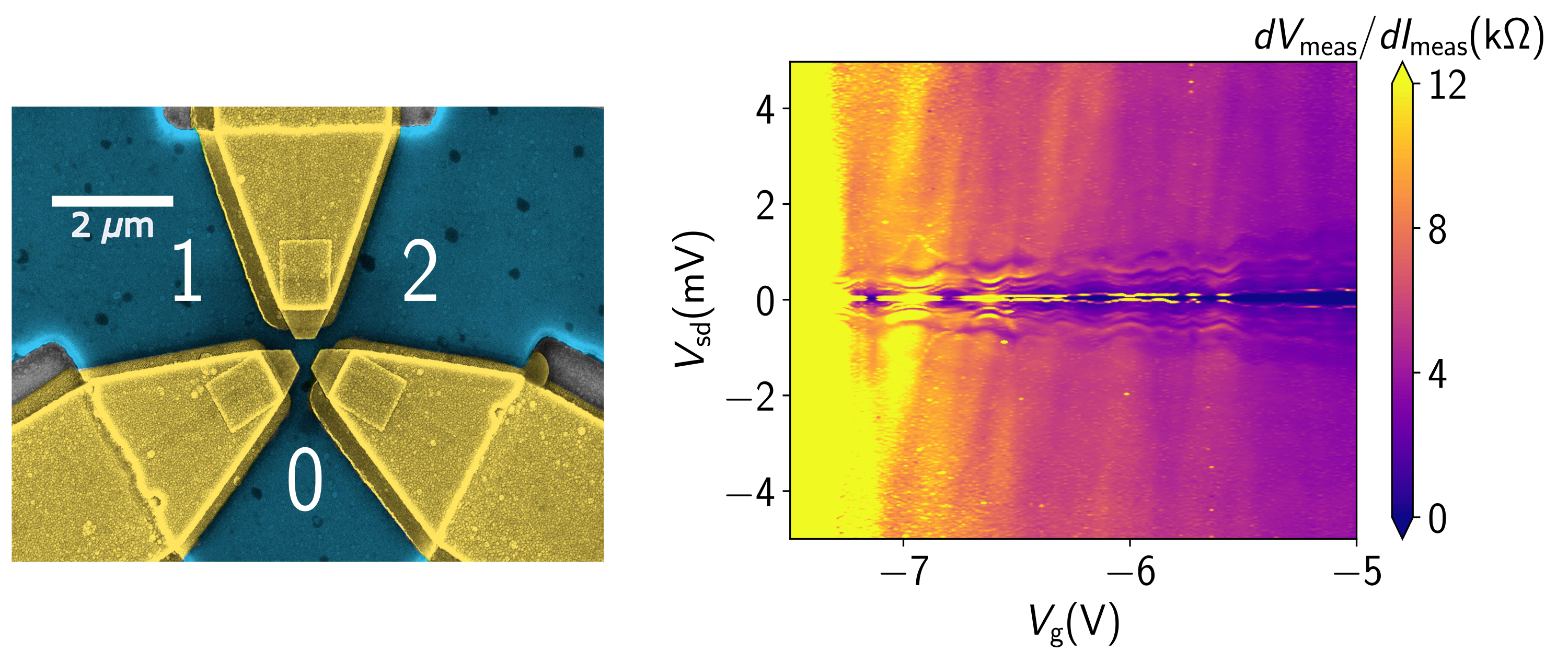
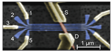
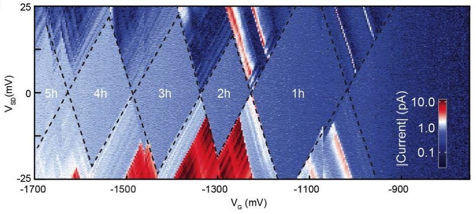
The Andreev bound state (ABS) spectra of Multi-terminal Josephson junctions (MTJJs) can form an artificial band structure in arbitrary dimensions. This ABS spectra is predicted to host topologically protected Weyl nodes and higher order Chern numbers [1,2]. The detection of these states require that the number of conductance modes hosted by the central scttering region is close to unity [3,4]. In our rece...
read more...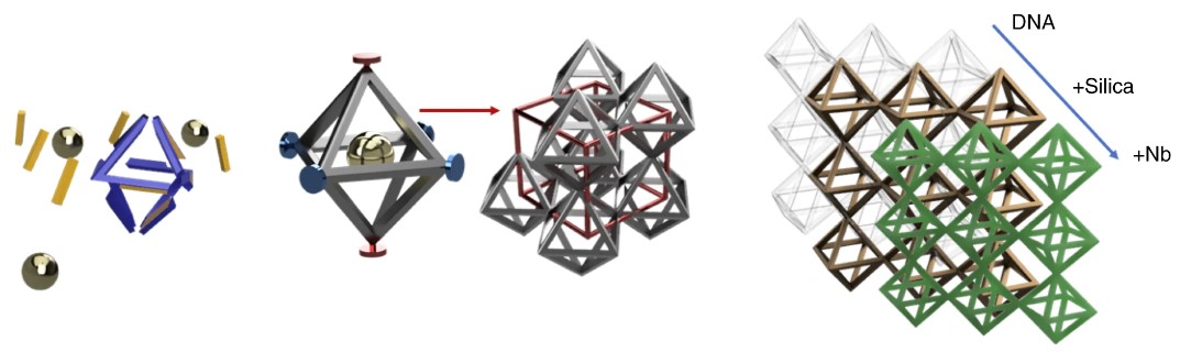
Self-assembled DNA [1] is a unique `bottom-up' fabrication method to create 1- 2- and 3-D structures with nanometric precision. The ability to create architecture that are not subjected to the limitation of conventional fabrication techniques i.e., e beam lithography, makes this technique appealing for nano- electronic applications. The major obstacles for integrating this technology in electronic circuit...
read more...